How Does a Transistor Work? The Tiny Switch That Built the Digital World
A transistor works by using a small electrical current or voltage to control the flow of a much larger current through a semiconductor material, acting as an electrically controlled switch or signal amplifier. This deceptively simple function, performed by a device smaller than a grain of sand, is the absolute foundation of modern electronics. By combining billions of transistors, we can create the logic gates, memory cells, and processors that form the brains of every computer, smartphone, and digital device. This article will demystify the physics behind the most common type—the Bipolar Junction Transistor (BJT)—and explain its role as the fundamental building block of the Information Age.
The Core Principle: Control and Amplification
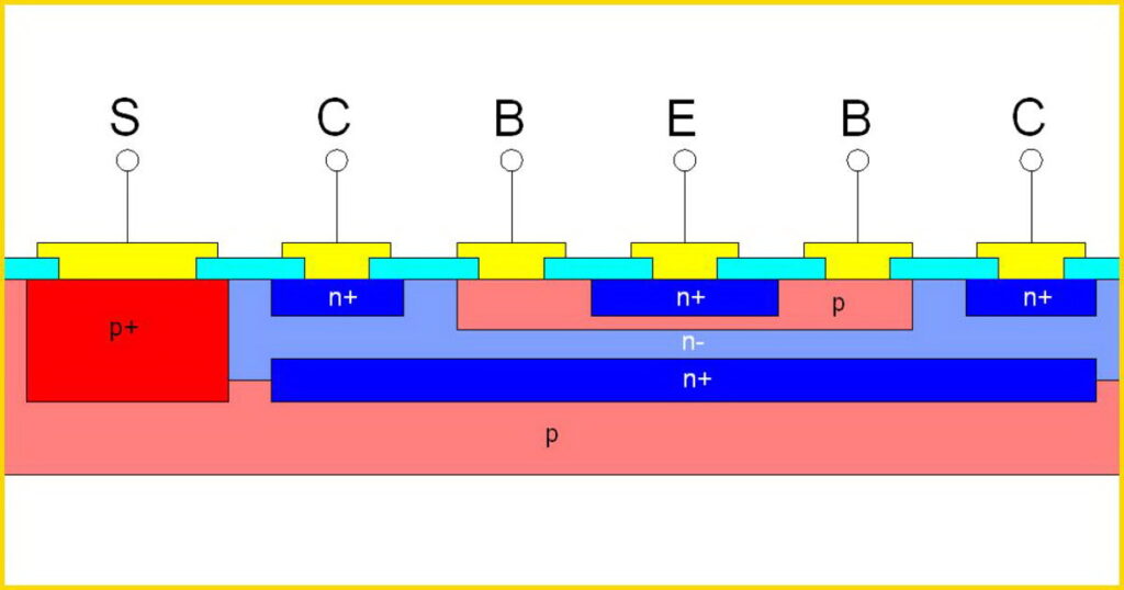
Imagine a valve on a water pipe. A tiny turn of the handle (small input) can control the flow of a huge volume of water (large output). A transistor does exactly this, but with electric current. It has three terminals:
- Input (Base): Where a small control current is applied.
- Output (Collector): Where the larger controlled current flows out.
- Common/Source (Emitter): The common reference point for the circuit.
This allows it to perform two critical functions:
- Switch: Turn a current fully ON or OFF (the basis of digital 1s and 0s).
- Amplifier: Make a weak signal stronger (essential for audio, radio, and sensors).
The Foundation: Semiconductors and Doping
To understand a transistor, you must first understand semiconductors, primarily silicon. A pure silicon crystal has a rigid atomic structure that doesn’t conduct electricity well—it’s an insulator. But we can engineer its conductivity through a process called doping.
- N-Type Silicon: Doped with atoms (like phosphorus) that have an extra electron. This creates a material with an excess of free, negatively charged carriers.
- P-Type Silicon: Doped with atoms (like boron) that have a «hole» (a missing electron). This creates a material with an excess of positively charged carriers (holes act like positive charges).
The magic happens at the junction where P-type and N-type materials meet.
Inside a Bipolar Junction Transistor (BJT)
The most intuitive type for beginners is the NPN transistor (there’s also a PNP). It’s like a silicon sandwich: a thin slice of P-type material (the Base) between two layers of N-type material (the Emitter and Collector).
💧 How It Works as a Switch: The «Water Valve» Analogy
How It Works as a Switch: The «Water Valve» Analogy
State 1: OFF (Switch Open)
- Condition: No small current applied to the Base.
- What happens: The junction between the Base (P) and Emitter (N) acts like a locked gate. No significant current can flow from the Collector to the Emitter, even if there’s a high voltage between them. The transistor is OFF, representing a binary 0.
State 2: ON (Switch Closed)
- Condition: A small positive current is applied to the Base.
- What happens: This base current «opens the gate.» It allows a much larger current to flood from the Collector, through the Base, and out the Emitter. The ratio of Collector current to Base current is the current gain (β or hFE), often 100 or more. A tiny control current (e.g., 0.01 mA) can switch a large load current (e.g., 1.0 mA). The transistor is ON, representing a binary 1.
This ON/OFF switching at billions of times per second is how computer processors perform calculations.
How It Works as an Amplifier: The «Signal Booster»
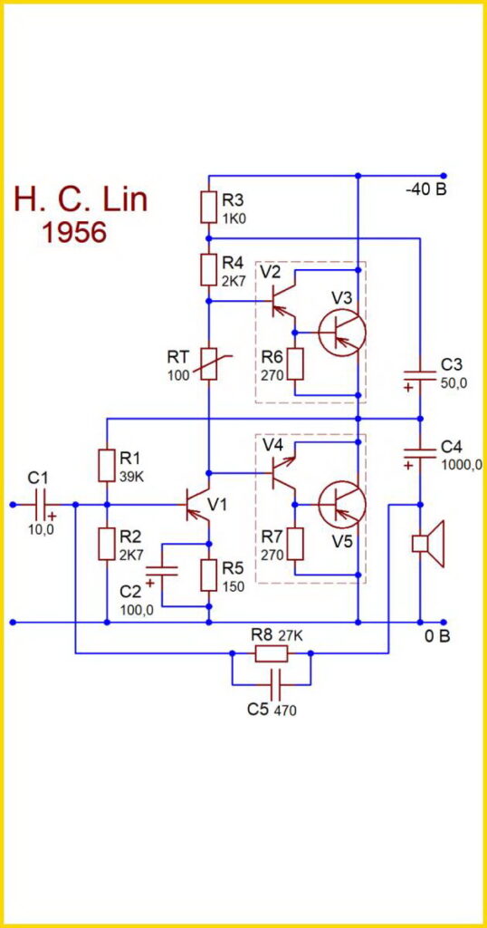
If we operate the transistor in its middle, active region (not fully ON or OFF), it can amplify.
- A tiny, fluctuating input signal (like a faint sound from a microphone) is applied to the Base.
- The transistor replicates the pattern of these fluctuations but at a much higher current strength drawn from the Collector’s power supply.
- The weak input signal thus controls a powerful output signal, amplifying it without changing its shape. This is how your stereo makes a weak audio file drive powerful speakers.
The MOSFET: The Transistor That Rules the Modern World
While the BJT is great for explanation, the most important transistor today is the Metal-Oxide-Semiconductor Field-Effect Transistor (MOSFET), which dominates computer chips.
Key Difference: A MOSFET is controlled by voltage, not current.
- Structure: It has a Gate (insulated by a tiny oxide layer), a Source, and a Drain.
- Operation: Applying a voltage to the Gate creates an electric field (hence «Field-Effect») that opens or closes a conductive channel between the Source and Drain. It’s like an electrostatic gate.
- Advantage: It uses virtually zero power to maintain its state (ON or OFF), which is why billions can be packed into a chip without it melting. This makes it perfect for digital logic and memory.
Why Transistors Changed Everything: From Vacuum Tubes to Microchips
Before transistors (circa 1947), we used vacuum tubes, which were bulky, fragile, power-hungry, and generated immense heat. A single early computer used thousands of tubes, filled entire rooms, and broke down constantly.
The solid-state transistor was a revolution:
- Small & Durable: Made of solid silicon.
- Low Power & Cool: Used little energy and produced little heat.
- Cheap & Scalable: Could be mass-produced and miniaturized.
This miniaturization led directly to the integrated circuit (IC) and microprocessor, enabling the personal computer, the internet, and the smartphone.
Frequently Asked Questions (FAQ)
How small are modern transistors?
Incredibly small. As of 2023-2024, cutting-edge chips (like Apple’s M-series or Intel’s Core Ultra) have transistors with features as small as 3 nanometers (nm). For scale, a human DNA helix is about 2.5 nm wide. Billions of these fit on a fingernail-sized chip.
What is «Moore’s Law»?
An observation (by Intel co-founder Gordon Moore) that the number of transistors on a microchip roughly doubles every two years, leading to exponential growth in computing power. While physical limits are now slowing this trend, it held true for over 50 years and drove the digital revolution.
Can you see a transistor?
Individual modern transistors are far smaller than the wavelength of visible light, so they are invisible to the naked eye and even to standard optical microscopes. They are fabricated and inspected using electron microscopes and other advanced tools.
What’s the difference between a transistor and a diode?
A diode is a simpler two-terminal device (P-N junction) that acts as a one-way valve for current. A transistor is a three-terminal device that uses this P-N junction principle to create a controllable valve or amplifier. You can think of a transistor as two diodes back-to-back, but with a crucial interactive effect in the middle layer.
(Conclusion)
The transistor is arguably the most important invention of the 20th century. By mastering the behavior of electrons in doped semiconductors, we created a device that could switch and amplify electrical signals with unparalleled efficiency and miniaturization. From the humble BJT to the voltage-controlled MOSFET, this tiny silicon switch replaced the clunky vacuum tube and became the fundamental logical unit of the digital world. Every click, swipe, calculation, and digital communication is, at its core, the orchestrated dance of billions of transistors turning on and off. Understanding the transistor is understanding the physical bedrock upon which our modern, connected reality is built.